Open-Circuit and Short-Circuit Loss Management in Wide-Gap Perovskite p-i-n Solar Cells
Feb 1, 2023·,, ,,,,,,,,,,,,,,·
0 min read
P. Caprioglio
Joel A. Smith
Robert D. J. Oliver
Akash Dasgupta
Saqlain Choudhary
Michael D. Farrar
A. Ramadan
Yen-Hung Lin
M. G. Christoforo
J. Ball
Jonas Diekmann
Jarla Thiesbrummel
Karl-Augustin Zaininger
Xinyi Shen
M. Johnston
D. Neher
M. Stolterfoht
H. Snaith

Abstract
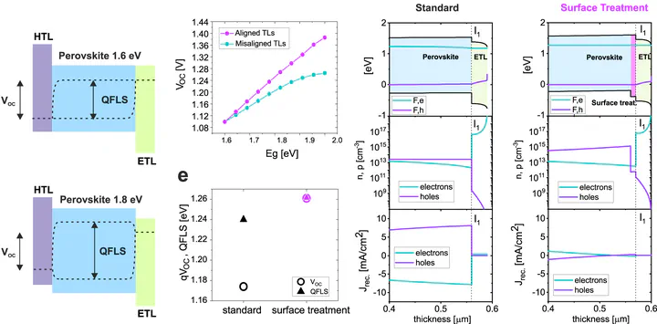
This work couples theoretical and experimental approaches to understand and reduce losses in wide-gap Br-rich perovskite p-i-n devices at open-circuit voltage (VOC) and short-circuit current (JSC) conditions. The study identifies a mismatch between the internal quasi-Fermi level splitting (QFLS) and the external VOC as detrimental. Surface modification of perovskites with guanidinium-Br and imidazolium-Br forms a low-dimensional phase at the n-interface, reducing this mismatch and boosting VOC. Ionic interlayers or self-assembled monolayers at the p-interface improve charge extraction and JSC by reducing field screening. These optimizations approach the thermodynamic potential of the perovskite absorber layer.
Type
Publication
Nature Communications